TYAN COMPUTER CORPORATION
S1952DLU
|
Device Type |
Mainboard |
|
Processor |
Pentium II |
|
Processor Speed |
350/400/450/500MHz |
|
Chip Set |
Intel 440GX |
|
Maximum Onboard Memory |
2GB (SDRAM supported) |
|
Cache |
256/512KB (located on Pentium II CPU) |
|
BIOS |
AMI |
|
Dimensions |
355mm x 304mm |
|
I/O Options |
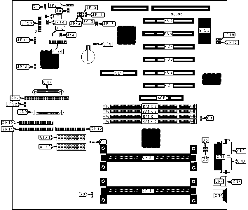
32-bit PCI slots (6), floppy drive interface, IDE interfaces (2), SCSI interface, Wide Ultra SCSI interfaces (2), parallel port, PS/2 mouse port, serial ports (2), IR connector, USB connectors (2), ATX power connector, AGP slot, RAID slot, wake on LAN connector, wake on modem connector |
|
CONNECTIONS | |||
|
Purpose |
Location |
Purpose |
Location |
|
AGP slot |
AGP |
IDE interface 1 |
CN10 |
|
ATX power connector |
ATX1 |
IDE interface 2 |
CN11 |
|
ATX power connector |
ATX2 |
Floppy drive interface |
CN12 |
|
Chassis fan power |
C1 |
Chassis intrusion connector |
J8 |
|
CPU fan power |
C2 |
Wake on LAN connector |
JP15 |
|
CPU fan power |
C3 |
Green PC connector |
JP17 |
|
Chassis fan power |
C4 |
Wake on modem connector |
JP19 |
|
CPU fan power |
C5 |
IDE interface LED |
JP20/pins 1 - 3 |
|
CPU fan power |
C6 |
Power LED |
JP20/pins 2 & 4 |
|
Parallel port |
CN1 |
Reset switch |
JP20/pins 5 & 7 |
|
Serial port 2 |
CN2 |
Soft off power supply |
JP20/pins 6 & 8 |
|
Serial port 1 |
CN3 |
IR connector |
JP20/pins 9 & 15 |
|
USB connector 1 |
CN4 |
SCSI interface LED |
JP27 |
|
USB connector 2 |
CN5 |
Server management connector |
JP28 |
|
PS/2 mouse port |
CN6 |
Speaker |
JP35 |
|
Wide Ultra SCSI interface |
CN7 |
32-bit PCI slots |
PC1 - PC6 |
|
SCSI interface |
CN8 |
RAID slot |
SL1 |
|
Wide Ultra SCSI interface |
CN9 | ||
|
USER CONFIGURABLE SETTINGS | |||
|
Function |
Label |
Position | |
|
» |
Factory configured - do not alter |
J14 |
Unidentified |
|
» |
Factory configured - do not alter |
J15 |
Unidentified |
|
» |
Factory configured - do not alter |
J17 |
Unidentified |
|
» |
Factory configured - do not alter |
JP2 |
Unidentified |
|
» |
CMOS memory normal operation |
JP3 |
Pins 1 & 2 closed |
|
CMOS memory clear |
JP3 |
Pins 2 & 3 closed | |
|
» |
Factory configured - do not alter |
JP21 |
Unidentified |
|
» |
Factory configured - do not alter |
JP22 |
Unidentified |
|
» |
Factory configured - do not alter |
JP23 |
Unidentified |
|
On board SCSI enabled |
JP36 |
Open | |
|
On board SCSI disabled |
JP36 |
Closed | |
|
Note: The location of JP2 & JP21 are unidentified. | |||
|
DIMM CONFIGURATION | ||||
|
Size |
Bank 0 |
Bank 1 |
Bank 2 |
Bank 3 |
|
8MB |
(1) 1M x 64 |
None |
None |
None |
|
16MB |
(1) 2M x 64 |
None |
None |
None |
|
16MB |
(1) 1M x 64 |
(1) 1M x 64 |
None |
None |
|
24MB |
(1) 2M x 64 |
(1) 1M x 64 |
None |
None |
|
24MB |
(1) 1M x 64 |
(1) 1M x 64 |
(1) 1M x 64 |
None |
|
32MB |
(1) 4M x 64 |
None |
None |
None |
|
DIMM CONFIGURATION (CON'T) | ||||
|
Size |
Bank 0 |
Bank 1 |
Bank 2 |
Bank 3 |
|
32MB |
(1) 2M x 64 |
(1) 2M x 64 |
None |
None |
|
32MB |
(1) 1M x 64 |
(1) 1M x 64 |
(1) 1M x 64 |
(1) 1M x 64 |
|
40MB |
(1) 4M x 64 |
(1) 1M x 64 |
None |
None |
|
48MB |
(1) 4M x 64 |
(1) 2M x 64 |
None |
None |
|
48MB |
(1) 2M x 64 |
(1) 2M x 64 |
(1) 2M x 64 |
None |
|
64MB |
(1) 2M x 64 |
(1) 2M x 64 |
(1) 2M x 64 |
(1) 2M x 64 |
|
64MB |
(1) 8M x 64 |
None |
None |
None |
|
64MB |
(1) 4M x 64 |
(1) 4M x 64 |
None |
None |
|
72MB |
(1) 8M x 64 |
(1) 1M x 64 |
None |
None |
|
80MB |
(1) 8M x 64 |
(1) 2M x 64 |
None |
None |
|
96MB |
(1) 8M x 64 |
(1) 4M x 64 |
None |
None |
|
96MB |
(1) 4M x 64 |
(1) 4M x 64 |
(1) 4M x 64 |
None |
|
128MB |
(1) 16M x 64 |
None |
None |
None |
|
128MB |
(1) 8M x 64 |
(1) 8M x 64 |
None |
None |
|
128MB |
(1) 4M x 64 |
(1) 4M x 64 |
(1) 4M x 64 |
(1) 4M x 64 |
|
136MB |
(1) 16M x 64 |
(1) 1M x 64 |
None |
None |
|
144MB |
(1) 16M x 64 |
(1) 2M x 64 |
None |
None |
|
176MB |
(1) 16M x 64 |
(1) 2M x 64 |
(1) 2M x 64 |
(1) 2M x 64 |
|
192MB |
(1) 16M x 64 |
(1) 8M x 64 |
None |
None |
|
192MB |
(1) 8M x 64 |
(1) 8M x 64 |
(1) 8M x 64 |
None |
|
256MB |
(1) 32M x 64 |
None |
None |
None |
|
256MB |
(1) 16M x 64 |
(1) 16M x 64 |
None |
None |
|
256MB |
(1) 8M x 64 |
(1) 8M x 64 |
(1) 8M x 64 |
(1) 8M x 64 |
|
272MB |
(1) 16M x 64 |
(1) 16M x 64 |
(1) 1M x 64 |
(1) 1M x 64 |
|
280MB |
(1) 32M x 64 |
(1) 1M x 64 |
(1) 1M x 64 |
(1) 1M x 64 |
|
288MB |
(1) 16M x 64 |
(1) 16M x 64 |
(1) 2M x 64 |
(1) 2M x 64 |
|
320MB |
(1) 16M x 64 |
(1) 16M x 64 |
(1) 4M x 64 |
(1) 4M x 64 |
|
384MB |
(1) 16M x 64 |
(1) 16M x 64 |
(1) 16M x 64 |
None |
|
448MB |
(1) 32M x 64 |
(1) 8M x 64 |
(1) 8M x 64 |
(1) 8M x 64 |
|
512MB |
(1) 64M x 64 |
None |
None |
None |
|
512MB |
(1) 32M x 64 |
(1) 32M x 64 |
None |
None |
|
512MB |
(1) 16M x 64 |
(1) 16M x 64 |
(1) 16M x 64 |
(1) 16M x 64 |
|
640MB |
(1) 32M x 64 |
(1) 16M x 64 |
(1) 16M x 64 |
(1) 16M x 64 |
|
768MB |
(1) 32M x 64 |
(1) 32M x 64 |
(1) 32M x 64 |
None |
|
1024MB |
(1) 64M x 64 |
(1) 64M x 64 |
None |
None |
|
1024MB |
(1) 32M x 64 |
(1) 32M x 64 |
(1) 32M x 64 |
(1) 32M x 64 |
|
1536MB |
(1) 64M x 64 |
(1) 64M x 64 |
(1) 64M x 64 |
None |
|
2048MB |
(1) 64M x 64 |
(1) 64M x 64 |
(1) 64M x 64 |
(1) 64M x 64 |
|
Note: Board accepts SDRAM memory. | ||||
|
CACHE CONFIGURATION |
|
Note: 256KB/512KB cache is located on the Pentium II CPU. |
|
CPU SPEED SELECTION | ||||||
|
CPU speed |
Clock speed |
Multiplier |
JP11 |
JP12 |
JP13 |
JP14 |
|
350MHz |
100MHz |
3.5x |
Closed |
Open |
Open |
Closed |
|
400MHz |
100MHz |
4x |
Open |
Closed |
Closed |
Closed |
|
450MHz |
100MHz |
4.5x |
Open |
Closed |
Open |
Closed |
|
500MHz |
100MHz |
5x |
Open |
Open |
Closed |
Closed |